Shuttling between science and invention
What we can learn from Bell Labs and the transistor
by Jason Crawford · May 27, 2020 · 7 min read
“The Link Between Science and Invention: The Case of the Transistor,” a 1962 paper by Richard Nelson at the RAND Corporation, provides a fascinating case study in invention at the frontiers of science, and the relation between the two. In it, we can see that research—and researchers—do not always fall neatly into categories like “basic” versus “applied,” nor is there a strict linear progression from one to the other.
First, some background. Engineers design electronic devices such as clocks, microwaves or computers by constructing electrical circuits out of a toolbox of basic components. One such component is the amplifier. An amplifier, as the name implies, produces an electrical output signal that is proportional to its input signal, but stronger.
Amplifiers are crucial for a number of applications. Long-distance communication lines depend on them, because when a signal travels along a very long wire it spreads out and gets “blurry”. Long-distance telegraph initially solved this problem through electromechanical “repeaters”, but long-distance telephone was effectively impossible. An amplifier can be used to build an electronic repeater that creates a fresh, sharp copy of the signal, say, every hundred miles. Amplifiers were also needed for radio broadcasting, to boost the small signal from a microphone into a large signal coming out of a radio tower. And in their “binary” form of an on/off switch, amplifiers are the basis of computers, enabling circuits that perform logical and mathematical operations on ones and zeros.
The first amplifier was based on the vacuum tube triode, invented by Lee de Forest in 1906. A glass tube was created with three electrodes: one connected to a filament, one to a plate, and one to a metal grid in between them. The tube was pumped empty. Electrons could jump through the vacuum from the filament to the plate, but a negative charge on the grid would stop them. The vacuum tube amplifier enabled cross-country telephone service in the 1910s, the radio industry in the 1920s, and the computer in the 1940s.
Vacuum tubes, however, were relatively large and ran hot. They are the reason that radios were once the size of cabinets, and that the first computer, made from some 18,000 tubes, took up an entire room. It was clear that a smaller, lighter, and less power-hungry amplifier would be valuable in a wide variety of devices. As the Bell Telephone Laboratories planned to return to peacetime research after World War II, the amplifier, among other potential inventions, was on their minds.
But how to create one? A promising technology was that of semiconductors.
Semiconductors are a class of materials. Some materials, such as metals, conduct electricity; others, such as rubber, do not. Semiconductors, such as germanium and silicon, do conduct electricity, but not as well as conductors. They are also distinguished by other properties. For instance, their electrical conductivity increases with temperature, the opposite of metals. And in particular, it was known at the time that some semiconductors passed current more easily in one direction than another. This action on the current is called “rectifying,” and a circuit component that does this is known as a rectifier.
Vacuum tubes, too, rectified current, and with the addition of a grid, they amplified it. It seemed reasonable, then, that semiconductors could somehow be made into amplifiers. Components made out of semiconducting material, rather than vacuum tubes, were called “solid-state”.
Motivated by this and other possibilities, Bell Labs set up a semiconductor research group in 1945 under William Shockley. They did not know from the outset exactly what they would be able to invent, only that the time was ripe for a major breakthrough, based on the understanding of semiconductor physics that had developed by the 1930s. Possible outcomes included rectifiers, thermistors, and photo-electric devices. Shockley, however, was optimistic about a solid-state amplifier, which would later be named the transistor.
Early approaches to the solid-state amplifier involved attempting to insert a grid into a semiconductor rectifier, the exact analogy to a vacuum tube amplifier, but these experiments did not work. The next idea was, in place of a grid, to impose an electric field on the material, a concept known as the field effect amplifier. This design was validated by Shockley’s calculations based on a theoretical model.
But what worked in theory failed in experiment. As Nelson describes it, “Sometimes even the sign of the effect was off. When the sign was right the magnitude of the effect was roughly a thousandth of the theoretical effect.”
To explain the failure of the theory, a new theory was needed:
[John] Bardeen proposed that the electrons affected by the field were not free inside the silicon, but were trapped at the surface in what he called surface states. Thus the application of an electric field would not significantly affect the number of free charge carriers in the semiconductor. Other scientists, including Shockley himself, had previously suggested the possibility of surface states at the free surface of a solid, but no one had realized the importance of this phenomenon to the properties of semiconductors.
Armed with an improved theory, the researchers continued their experiments in an attempt to find “a way to neutralize the surface states so that a useful field effect amplifier could be built.” In one such experiment,
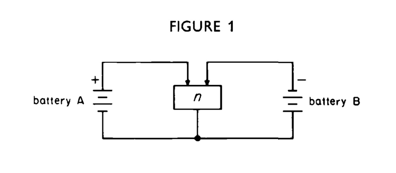
two contacts were placed quite close together on a germanium crystal. (Figure 1). It does not matter here just why this particular experiment was performed. What is significant is that it was not performed with the hope of observing the most important result it yielded.

The result it yielded was an amplification effect—exactly what the researchers were trying to achieve—but through a different mechanism than they were expecting. This was not a field effect amplifier. It became known as the “point contact” transistor. But how did it work? In the first instance, new theory was needed to explain an experimental failure. Now, new theory was needed to explain an unexpected success.
By this time it was understood that there were two types of semiconductors. Negative or “n-type” semiconductors have an excess of electrons; the motion of the extra electrons through them carries the current. Positive or “p-type” semiconductors have empty spots where electrons could be, but aren’t, called “holes”. As electrons jump backwards to fill the holes, the effect is the same as that of a positive charge moving forwards, and so we speak of the holes as “moving” and “carrying” charge.
What was not fully appreciated at the time was that it is also possible for electrons to flow through p-type semiconductors, and conversely for holes to “flow” through n-type. This part of the theory, a phenomenon known as “minority carriers”, explained the working of the point-contact transistor: holes were flowing between the two contacts.
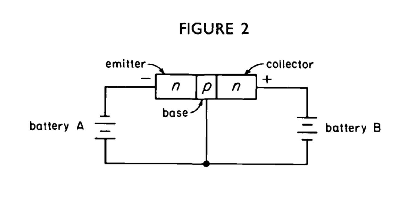
The point-contact transistor, though, was soon superseded by a new design. The idea of minority carriers enabled Shockley to theorize a new type of transistor, the junction transistor. In this design, a thin layer of p-type material, for instance, sits between two blocks of n-type. A voltage applied to the p region allows a current to flow through it, from one n region to the other. Within the p region, the electrons in that current are minority carriers.

This time, theory matched practice. The junction transistor worked—making possible compact radios, satellites, and ultimately the smartphone in your pocket.
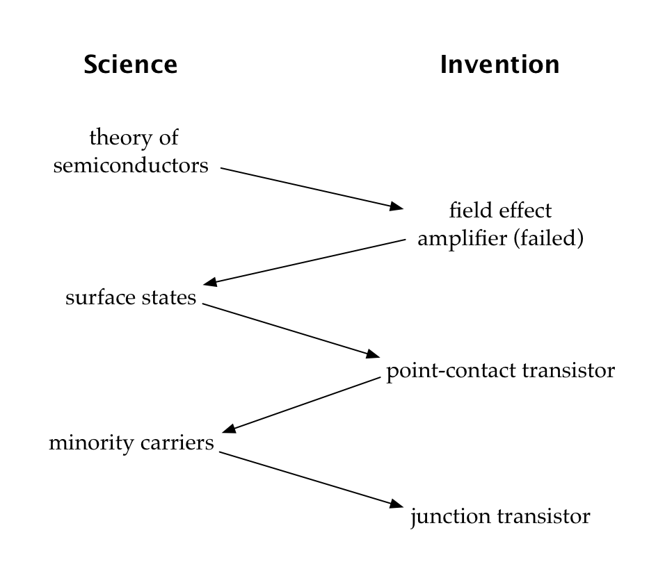
What I find fascinating about this story is the shuttling up and down the ladder of abstraction, from scientific theory to practical invention and back again. Diagrammatically, the timeline of invention looks like this:

One aspect of this is that inventing the transistor required new discoveries in physics. Although the existing theory of semiconductors provided an indispensable starting point, further refinement of the theory was needed. The transistor could not, in the 1940s, have been created by inventors who were either unable or unwilling to act as scientists when necessary.
Conversely, the science of semiconductor physics was driven forward in the process of invention. Despite extensive research into semiconductors, physicists had not explored issues such as surface states or minority carriers in sufficient depth for the work at Bell Labs. The process of invention, possessing a different set of goals and incentives than that of pure science, led in different directions that highlighted new phenomena. The result was not only an invention, but an advance in knowledge.
Thus, both science and engineering profited from the existence of a laboratory where researchers were willing and able to cycle back and forth between discovery and invention. What does such a lab require?
First, it requires researchers who are capable of both: inventors who are also trained as scientists. Even more, it requires them to be motivated by both. Shockley, Bardeen, and Walter Brattain, who shared a Nobel Prize for the transistor in 1956, were this kind of researcher.
It also requires the work environment to be supportive of both. If in a corporate lab, as in this case, management must approve of researchers exploring scientific questions, even if it’s unclear how long this will take or whether it will ever result in profitable inventions. If in a nonprofit environment such as a university, the incentive structure must not discourage the pursuit of practical applications, even if this comes at the expense of theoretical work.
Further, the researchers must have a large degree of freedom in the focus and direction of their work. As experiments proceed and certain paths and approaches grow more or less promising, they must be able to respond rapidly to the shifting information landscape. Nelson draws an analogy to entrepreneurs in a market economy, and says that researchers need to be free to follow their intuition of “scientific promise” (which, like all intuitions, cannot always be justified to others except in retrospect). Another implication is that researchers cannot be held to any kind of tight timeline on which they are to achieve results.
How then are researchers to be managed? Nelson describes a process in which researchers are free to explore new areas on their own. If their initial work proves promising, more resources may be devoted to the area. If not,
eventually the individual in question will be requested to return to the fold, or leave. It is hoped that pressure can be informal. There seems to be no consensus about how long to let a man wander, but it is clear that young and newly hired scientists are kept under closer reins than the more senior scientists. However, even top-flight people, like [Karl] Jansky, have been asked to change their line of research. But, in general, the experience has been that informal pressures together with the hiring policy are sufficient to keep AT&T and Western Electric more than satisfied with the output of research.
I don’t think the transistor is an isolated case. Something similar happened when James Watt was working to improve the efficiency of the steam engine (although in that case, the relevant physics—latent heat—already existed; Watt simply didn’t know about it before he essentially rediscovered it). I believe there is a similar story behind the invention of nylon by Wallace Carothers at DuPont.
If this type of invention, with frequent “dips” into science, is important—and the transistor was extremely important—then it’s worth considering whether it is supported well by our current models of funding and managing research.
